Showing posts with label transistor. Show all posts

Thursday, September 2, 2010

170W Audio Power Amplifier.


Download this schematic diagram.

Download part list component.


Datasheet semiconductor component.

1. NE5534

2. MJE350

3. MJE340

4. BD139

5. BC546B

6. BC556B

7. MJE15030

8. MJE15031

9. MJE15003

10. MJE15004

11. BAT85

12. IN4004

13. BY254

The circuit is being powered by two 15V power supply for each channel, that is regulated by the combination of resistors R7-9 and Zener diodes D1-2. The frequency bandwidth is limited to a specific value due to the presence of low pass filter from R2 & C2 and high pass filter from R3 & C1. The total feedback of the circuit is concentrated on the positive non-inverting input of the IC1 that functions as differential amplifier. The node of R4-5 is applied with the feedback voltage from the output through R6. The current regulated by R10 & R14 across Q1-2 is 10mA as they operate in class A while in class AB, the power transistors Q8-11 operate in the output with a regulated constant current of 100mA each power transistor, done by trimmer TR1 and Q3. This will match the voltage drop at 27mV, higher than the provided voltage of R25-28.

A heatsink with sufficient dimension to provide cooling is placed above Q1-2-3-6-7 to maintain the possible thermic stability while the protection from reverse voltages from the load is performed by diodes D9-10.Additional fan can also be employed to suppress high temperature for efficient operation. The stability during high frequencies is sustained by the Zobel network consisting of R29 & C18. Due to capacitive load, the amplifier output is protected by a 1mm diameter 15-coil inductor L1 with R30 for square pulses passage.

Each power amplifier that is created will correspond to a transformer to handle large capacitors and provide proportional power. The transformer input is connected to the AC line which can incorporate delay circuit for protection from excessive supply. The cables that would carry the current to the amplifier should be appropriate enough.

Wednesday, September 1, 2010

1000 W Power Amplifier Schematic Diagram.


Download this schematic diagram.


Datasheet semiconductor component download.

1. BC546
2. BD681
3. MJE350
4. MJE340
5. 2SC5200
6. 2SA1943
7. 2SA1494
8. 2SC3858


200W ATX PC Power Supply Electronic Circuit.


Download this schematic diagram.


Datasheet semiconductor component. (PDF Format)

1. IN5406
2. 2SC4242
3. FR155
4. 2SC945
5. 2SA733
6. 2SC3457
7. LM7805
8. TL494
9. LM393
10. TL431C

Here I bring you wiring diagram of PCs power supply of DTK company. This power supply has ATX design and 200W performance. I was drawed diagram, when I repaired this power supply.

This power supply circuit uses chip TL494. Similar circuit is used in the most power supplies with output power about 200W.Device use push-pull transistor circuit with regulation of output voltage.

Line voltage goes through input filter circuit (C1, R1, T1, C4, T5) to the bridge rectifier. When voltage is switched from 230V to 115V, then rectifier works like a doubler. Varistors Z1 and Z2 have overvoltage protect function on the line input.
Thermistor NTCR1 limits input current until capacitors C5 and C6 are charged. R2 and R3 are only for discharge capacitors after disconnecting power supply. When power supply is connected to the line voltage, then at first are charged capacitors C5 and C6 together for about 300V.
Then take a run secondary power supply controlled by transistor Q12 and on his output will be voltage. Behind the voltage regulator IC3 will be voltage 5V, which goes in to the motherboard and it is necessary for turn-on logic and for "Wake on something" functions.
Next unstabilized voltage goes through diode D30 to the main control chip IC1 and control transistors Q3 and Q4. When main power supply is running, then this voltage goes from +12V output through diode D.

Tuesday, August 31, 2010

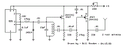
88-108 MHz FM Broadcast Transmitter Circuit.


Download this schematic diagram.


Datasheet semiconductor component.

1. NE555
2. 2N4392

This circuit will transmit a continuous audio tone on the FM broadcast band (88-108 MHz) which could used for remote control or security purposes. Circuit draws about 30 mA from a 6-9 volt battery and can be
received to about 100 yards. A 555 timer is used to produce the tone (about 600 Hz) which frequency modulates a Hartley oscillator. A second JFET transistor buffer stage is used to isolate the oscillator from the antenna so that the antenna position and length has less effect on the frequency. Fine frequency adjustment can be made by adjusting the 200 ohm resistor in series with the battery. Oscillator frequency is set by a 5 turn tapped inductor and 13 pF capacitor. The inductor was wound around a #8 X 32 bolt (about 3/16 diameter) and then removed by unscrewing the bolt. The inductor was then streached to about a 3/8 inch length and tapped near the center. The oscillator frequency should come out somewhere near the center of the band (98 MHz) and can be shifted higher or lower by slightly expanding or compressing the inductor. A small signal diode (1N914 or 1N4148) is used as a varactor diode so that the total capacity in parallel with the inductor varies slightly at the audio rate thus causing the oscillator frequency to change at the audio rate (600 Hz). The ramping waveform at pins 2 and 6 of the timer is applied to the reversed biased diode through a large (1 Meg) resistor so that the capacitance of the diode changes as the ramping voltage changes thus altering the frequency of the tank circuit. Alternately, an audio signal could be applied to the 1 Meg resistor to modulate the oscillator but it may require an additional pullup resistor to reverse bias the diode. The N channel JFET transistors used should be high frequency VHF or UHF types (Radio Shack #276-2062 MPF102) or similar.

Wednesday, May 20, 2009

LM317T Voltage Regulator with Pass Transistor

The LM317T output current can be increased by using an additional power transistor to share a portion of the total current. The amount of current sharing is established with a resistor placed in series with the 317 input and a resistor placed in series with the emitter of the pass transistor.


Download this schematic.


Download list datasheet semiconductor parts. (PDF Format)

1. 2N2955
2. LM317A
3. IN4002

http://www.circuits-lab.com/

Monday, April 13, 2009

15 Watt Mini Amplifier

A 15 watt amplifier made using discrete components. Sergio designed this circuit for his Electronics Level II course.


Download this schematic diagram.


Download list datasheet semiconductor component. (PDF Format)

1. 2N3904
2. 2N2907A
3. 2N3906
4. IN4002


Notes:
This amplifier uses a dual 20 Volt power supply and delivers 15 watts RMS into an 8 ohm load. Q1 operates in common emitter, the input signal being passed to the bias chain consisting of Q8, Q9, D6, D13 and D14. Q8 and Q9 provide a constant current through the bias chain to minimize distortion, the output stage formed by a discrete darlington pair (Q2,Q4) and (Q7,Q11). The last two transistors are power Transitors, specifically the 2N3055 and MJ2955. The 7.02K resistor, R16 was made using a series combination of a 4.7K, 680 Ohms, and two 820 Ohms. The 1.1K resistor, R3 was made using a 100 Ohms and a 1K resistor. You can use this circuit with any walkman or CD player since it is designed to take a standard 500mv RMS signal.


http://www.zen22142.zen.co.uk/

Thursday, March 12, 2009

Transistorized Inverter 60W 12V DC to 230V AC


Download this schematic.


Download datasheet semiconductor component. (PDF Format)

1. BC548
2. BD140
3. 2N6107
4. 2N3055

This is low cost fully transistorised inverter circuit capable of driving medium loads of the order of 40 to 60 watts using battery of 12V, 15 Ah or higher capacity.

Transistors T1 and T2 (BC548) form a 50Hz multivibrator. For obtaining correct frequency, the values of resistors R3 and R4 may have to be changed after testing. The complementary outputs from collectors of transistors T1 and T2 are given to PNP darlington driver stages formed by transistor pairs T3-T4 and T6-T7 (utilising transistors BD140 and 2N6107). The outputs from the drivers are fed to transistors T5 and T8 (2N3055) connected for push-pull operation.

Somewhat higher wattage can be achieved by increasing the drive to 2N3055 transistors (by lowering the value of resistors R7 and R8 while increasing their wattage). Suitable heatsinks may be used for the output stage transistors. Transformer X1 is a 230V primary to 9V-0-9V, 10A secondary used in reverse.