Monday, April 20, 2009

12 Volt 30 Amp Power Supply


Download this schematic diagram.


Download list datasheet semiconductor parts. (PDF Format)

1. TIP2955
2. LM7812


Description

Using a single 7812 IC voltage regulator and multiple outboard pass transistors, this power supply can deliver output load currents of up to 30 amps. The design is shown below:

The input transformer is likely to be the most expensive part of the entire project. As an alternative, a couple of 12 Volt car batteries could be used. The input voltage to the regulator must be at least several volts higher than the output voltage (12V) so that the regulator can maintain its output. If a transformer is used, then the rectifier diodes must be capable of passing a very high peak forward current, typically 100amps or more. The 7812 IC will only pass 1 amp or less of the output current, the remainder being supplied by the outboard pass transistors. As the circuit is designed to handle loads of up to 30 amps, then six TIP2955 are wired in parallel to meet this demand. The dissipation in each power transistor is one sixth of the total load, but adequate heat sinking is still required. Maximum load current will generate maximum dissipation, so a very large heat sink is required. In considering a heat sink, it may be a good idea to look for either a fan or water cooled heat sink. In the event that the power transistors should fail, then the regulator would have to supply full load current and would fail with catastrophic results. A 1 amp fuse in the regulators output prevents a safeguard. The 400mohm load is for test purposes only and should not be included in the final circuit.

for detail, pleace click here

0 - 300V Adjustable Power Supply.


Download this schematic.


Download datasheet semiconductor parts. (PDF Format)

1. BUZ326
2. BC547

Introduction

To prevent my high voltage experiments to go up in smoke completely, I designed
a simple circuit which can provide an adjustable voltage source of 0 to 330 Volt..
The supply is short-ciruit proof: the current is limited to about 100mA.

Circuit description

TR1 is a 1:1 mains transformer; it is included for safety.

The mains voltage from TR1 is rectified with bridge D1 (1Amp / 500V) and large elcap C1.

T1 is switched as a source follower: the source of T1 will follow the voltage of the
wiper of R3. D2 is included to protect the gate of T1; although in theory not necessary
I strongly recommend to include it!

T2 and shunt resistor R2 build the current limiter. When the output current becomes too high, T2 will discharge
the gate of T1. This will prevent the current to become too high.
The value of R3 has been determined experimentally; it depends also on the Hfe of T2 so you may need to tune the value of R2.

Note that T1 needs a large heatsink: in worst case T1 will dissipate 330V x 100mA = 33Watt!
Instead of a BUZ 326 (400V/10.5Amp) you can also use an IRF740 (400V/10Amp).
The output impedance of the power supply is determined by the beta of T1, so the larger the MOSFET
the lower the output impedance!


Monday, April 13, 2009

15 Watt Mini Amplifier

A 15 watt amplifier made using discrete components. Sergio designed this circuit for his Electronics Level II course.


Download this schematic diagram.


Download list datasheet semiconductor component. (PDF Format)

1. 2N3904
2. 2N2907A
3. 2N3906
4. IN4002


Notes:
This amplifier uses a dual 20 Volt power supply and delivers 15 watts RMS into an 8 ohm load. Q1 operates in common emitter, the input signal being passed to the bias chain consisting of Q8, Q9, D6, D13 and D14. Q8 and Q9 provide a constant current through the bias chain to minimize distortion, the output stage formed by a discrete darlington pair (Q2,Q4) and (Q7,Q11). The last two transistors are power Transitors, specifically the 2N3055 and MJ2955. The 7.02K resistor, R16 was made using a series combination of a 4.7K, 680 Ohms, and two 820 Ohms. The 1.1K resistor, R3 was made using a 100 Ohms and a 1K resistor. You can use this circuit with any walkman or CD player since it is designed to take a standard 500mv RMS signal.


http://www.zen22142.zen.co.uk/

100W Guitar Power Amplifier

The power amp board has remained unchanged since it was first published in 2002. It certainly isn't broken, so there's no reason to fix it. The photo below shows a fully assembled board (available as shown as M27). Using TIP35/36C transistors, the output stage is deliberately massive overkill. This ensures reliability under the most arduous stage conditions. No amplifier can be made immune from everything, but this does come close.


Download this image.


The power amp (like the previous version) is loosely based on the 60 Watt amp previously published (Project 03), but it has increased gain to match the preamp. Other modifications include the short circuit protection - the two little groups of components next to the bias diodes (D2 and D3). This new version is not massively different from the original, but has adjustable bias, and is designed to provide a "constant current" (i.e. high impedance) output to the speakers - this is achieved using R23 and R26. Note that with this arrangement, the gain will change depending on the load impedance, with lower impedances giving lower power amp gain. This is not a problem, so may safely be ignored.

Should the output be shorted, the constant current output characteristic will provide an initial level of protection, but is not completely foolproof. The short circuit protection will limit the output current to a relatively safe level, but a sustained short will cause the output transistors to fail if the amp is driven hard. The protection is designed not to operate under normal conditions, but will limit the peak output current to about 8.5 Amps. Under these conditions, the internal fuses (or the output transistors) will probably blow if the short is not detected in time.


Download this schematic diagram.


Download datasheet semiconductor component. (PDF Format)

1. BC559

2. BC549

3. BD139

4. BD140

5. TIP35C

6. TIP36C


Guitar Pre-Amplifier

A photo of the Revision-A preamp is shown below. You'll see that there are two dual opamps, but the schematic only shows one. This is the main part of the Rev-A update - the output section now has gain (which is easily selected), and a better buffered low output impedance. The remainder of the circuit is unchanged. Full details of the new version are available on the secure site for those who purchase the PCBs.


Download this image.


The preamp circuit is shown in Figure 1, and has a few interesting characteristics that separate it from the "normal" - assuming that there is such a thing. This is simple but elegant design, that provides excellent tonal range. The gain structure is designed to provide a huge amount of gain, which is ideal for those guitarists who like to get that fully distorted "fat" sound.

However, with a couple of simple changes, the preamp can be tamed to suit just about any style of playing. Likewise, the tone controls as shown have sufficient range to cover almost anything from an electrified violin to a bass guitar - The response can be limited if you wish (by experimenting with the tone control capacitor values), but I suggest that you try it "as is" before making any changes.


Download this schematic diagram.


semiconductor datasheet component. (PDF Format)

1. TL072
2. BC549


Automatic Loudness Control


In order to obtain a good audio reproduction at different listening levels, a different tone-controls setting should be necessary to suit the well known behaviour of the human ear. In fact, the human ear sensitivity varies in a non-linear manner through the entire audible frequency band, as shown by Fletcher-Munson curves.
A simple approach to this problem can be done inserting a circuit in the preamplifier stage, capable of varying automatically the frequency response of the entire audio chain in respect to the position of the control knob, in order to keep ideal listening conditions under different listening levels.
Fortunately, the human ear is not too critical, so a rather simple circuit can provide a satisfactory performance through a 40dB range.
The circuit is shown with SW1 in the "Control-flat" position, i.e. without the Automatic Loudness Control. In this position the circuit acts as a linear preamplifier stage, with the voltage gain set by means of Trimmer R7.
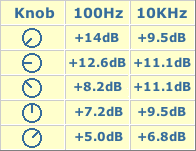
Switching SW1 in the opposite position the circuit becomes an Automatic Loudness Control and its frequency response varies in respect to the position of the control knob by the amount shown in the table below.
C1 boosts the low frequencies and C4 boosts the higher ones. Maximum boost at low frequencies is limited by R2; R5 do the same at high frequencies.

Technical data:

Frequency response referred to 1KHz and different control knob positions:

Knob position table

Total harmonic distortion at all frequencies and 1V RMS output: <0.01%

Notes:

  • SW1 is shown in "Control flat" position.
  • Schematic shows left channel only, therefore for stereo operation all parts must be doubled except IC1, C6 and C8.
  • Numbers in parentheses show IC1 right channel pin connections.
  • R7 should be set to obtain maximum undistorted output power from the amplifier with a standard music programme source and P1 rotated fully clockwise.

9v Battery Voltage Monitor using a LTC1440 Comparator

This circuit turns on a LED whenever the voltage of a standard 9v battery connected to the circuit drops below 7.2 volts. It uses a LTC1440 comparator, which also contains a 1.18v reference diode. In standby mode, the circuit draws only 4uA.


Battery Monitor Circuits
Master Schematic Category List - David A. Johnson, P.E.


Friday, April 10, 2009

120 VAC Lamp Dimmer

The full wave phase control circuit below was found in a RCA power circuits book from 1969. The load is placed in series with the AC line and the four diodes provide a full wave rectified voltage to the anode of a SCR. Two small signal transistors are connected in a switch configuration so that when the voltage on the 2.2uF capacitor reaches about 8 volts, the transistors will switch on and discharge the capacitor through the SCR gate causing it to begin conducting. The time delay from the beginning of each half cycle to the point where the SCR switches on is controlled by the 50K resistor which adjusts the time required for the 2uF capacitor to charge to 8 volts. As the resistance is reduced, the time is reduced and the SCR will conduct earlier during each half cycle which applies a greater average voltage across the load. With the resistance set to minimum the SCR will trigger when the voltage rises to about 40 volts or 15 degrees into the cycle. To compensate for component tollerances, the 15K resistor can be adjusted slightly so that the output voltage is near zero when the 50K pot is set to maximum. Increasing the 15K resistor will reduce the setting of the 50K pot for minimum output and visa versa. Be careful not to touch the circuit while it is connected to the AC line.


visit: http://www.discovercircuits.com/list.htm

Variable Voltage and Current Power Supply


Download this schematic.


Download list datasheet semiconductor parts. (PDF Format)

1. 2N3055
2. LM1458

Another method of using opamps to regulate a power supply is shown below. The power transformer requires an additional winding to supply the op-amps with a bipolar voltage (+/- 8 volts), and the negative voltage is also used to generate a reference voltage below ground so that the output voltage can be adjusted all the way down to 0. Current limiting is accomplished by sensing the voltage drop across a small resistor placed in series with the negative supply line. As the current increases, the voltage at the wiper of the 500 ohm pot rises until it becomes equal or slightly more positive than the voltage at the (+) input of the opamp. The opamp output then moves negative and reduces the voltage at the base of the 2N3053 transistor which in turn reduces the current to the 2N3055 pass transistor so that the current stays at a constant level even if the supply is shorted. Current limiting range is about 0 - 3 amps with components shown. The TIP32 and 2N3055 pass transistors should be mounted on suitable heat sinks and the 0.2 ohm current sensing resistor should be rated at 2 watts or more. The heat produced by the pass transistor will be the product of the difference in voltage between the input and output, and the load current. So, for example if the input voltage (at the collector of the pass transistor) is 25 and the output is adjusted for 6 volts and the load is drawing 1 amp, the heat dissipated by the pass transistor would be (25-6) * 1 = 19 watts. In the circuit below, the switch could be set to the 18 volt position to reduce the heat generated to about 12 watts.


http://www.discovercircuits.com/list.htm

Variable 3 - 24 Volt / 3 Amp Power Supply

This regulated power supply can be adjusted from 3 to 25 volts and is current limited to 2 amps as shown, but may be increased to 3 amps or more by selecting a smaller current sense resistor (0.3 ohm). The 2N3055 and 2N3053 transistors should be mounted on suitable heat sinks and the current sense resistor should be rated at 3 watts or more. Voltage regulation is controlled by 1/2 of a 1558 or 1458 op-amp. The 1458 may be substituted in the circuit below, but it is recommended the supply voltage to pin 8 be limited to 30 VDC, which can be accomplished by adding a 6.2 volt zener or 5.1 K resistor in series with pin 8. The maximum DC supply voltage for the 1458 and 1558 is 36 and 44 respectively. The power transformer should be capable of the desired current while maintaining an input voltage at least 4 volts higher than the desired output, but not exceeding the maximum supply voltage of the op-amp under minimal load conditions. The power transformer shown is a center tapped 25.2 volt AC / 2 amp unit that will provide regulated outputs of 24 volts at 0.7 amps, 15 volts at 2 amps, or 6 volts at 3 amps. The 3 amp output is obtained using the center tap of the transformer with the switch in the 18 volt position. All components should be available at Radio Shack with the exception of the 1558 op-amp.


Download this schematic.


Download datasheet semiconductor component. (PDF Format)

1. 2N3055
2. 2N3053
3. 2N3904
4. LM1558

Sunday, April 5, 2009

0-30V Stabilized Variable Power Supply with Current Control


This is high quality stabilized power supply circuit diagram. You will able to adjust the output voltage from 0 volt up to 30 volt DC. You also able to adjust the current output value from 0.002 A to 3 A.

Detail explanation include the PCB layout, visit this page

Flashing Heart Circuit

This is LED flashing circuit, the circuit is quite simple. Alternatively, you could be create another shape, not just heart shape.


Download this schematic.


Component list:

Resistors
R1, R2 - 470 ohm, 1/2-watt
R3-R5 - 100 ohm, 3-watt
R6-R8 - 1000 ohm, 1.4-watt
R9 - 5000 ohm potentiometer


Capacitors
C1, C2 - 100uF, 16 volts, electrolytic radial


Semiconductors
IC1 - 4047, low power monostable/astable multivibrator
Q1-Q3 - 2n3643 NPN transistor or equivalent

Download datasheet
semiconductor
component:

1. 4047
2. 2N3643


Diodes

LED1-LED84 - yellow light-emitting diode
LED85-LED126 - red light-emitting diode
LED127-LED142 - green light-emitting diode


Other components
PS1 - 12VDC @ 500mA wall transformer


Miscellaneous: Jumper wire, solder, printed circuit board,
drill and bits,14 pin I.C. socket, and a frame or case.

Capacitor Explanation

A capacitor is a passive electrical component that can store energy in the electric field between a pair of conductors (called "plates"). The process of storing energy in the capacitor is known as "charging", and involves electric charges of equal magnitude, but opposite polarity, building up on each plate. A capacitor's ability to store charge is measured by its capacitance, in units of farads.

Capacitors are often used in electric and electronic circuits as energy-storage devices. They can also be used to differentiate between high-frequency and low-frequency signals. This property makes them useful in electronic filters. Practical capacitors have series resistance, internal leakage of charge, series inductance and other non-ideal properties not found in a theoretical, ideal, capacitor.

The capacitor is used in almost every electronic circuit. It is a very important component and it does many different things, depending on where it is placed.

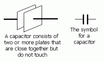
A capacitor is basically a device that stores a charge of electricity.
It has two or more plates that are separated by air or a non conducting medium such as plastic.

A basic capacitor is shown in the diagram below with the corresponding circuit symbol.
Capacitor Explanation
Capacitors can be large or small and the size is the result of the value of the capacitor as well as the voltage it is capable of withstanding.

There is a lot to learn about capacitors and we will only be discussing the very basics.
There are many types of capacitors, here are 5 of the most common types:

AIR - such as a tuning capacitor in a radio.

GREENCAP - a polyester capacitor.

CERAMIC - a ceramic insulating material that produces a very compact
capacitor

MONOBLOCK - also called monolithic - a multi-cceramic capacitor

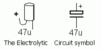
ELECTROLYTIC - aluminium plates with a moist insulating medium. This type of capacitor has a very high capacitance in a small space.

The diagram below shows a single-ended electrolytic, suitable for mounting on a printed circuit board and the symbol.
electrolytic capacitor
The unit for capacitance is the FARAD. But one Farad is an enormous value and we don't use values this large in electronics. The value we use is the micro-farad. A microfarad is one-millionth of a farad.

For some circuits we need capacitors of more than 1 microfarad capacitance and for others we need less than 1 microfarad.

For a power supply we need electrolytics of 10 microfarad, 100 microfarad, 1,000 microfarad and even 10,000 microfarad. The letter to signify microfarad is "uF" or simply "u". Thus 1microfarad is 1u, 10 microfarad is 10u etc.

For audio work we need smaller values such as .1microfarad and .01 microfarad.
In electronics, we try and avoid using the decimal point as it can be rubbed off components and omitted from photocopies of circuit diagrams.

To get around this we use sub-multiples and the sub-multiple of microfarad is nanofarad.

1,000 nanofarad = 1 microfarad.
Thus .1u = 100 nanofarad.
The letter to represent nanofarad is "n".
Thus .01u = 10n

For radio frequency work, even smaller values of capacitance are needed.

The nanofarad is divided into 1,000 parts called picofarad. Thus 1,000 picofarad = 1nanofarad.

The picofarad is written pF or simply "p."
Thus 1,000p = 1n.

Some capacitors are physically very small and there is very little space to write the component value. To get around this, manufacturers have produced a numbering system using 3 digits.

It is based on picofarads. A 100 picofarad capacitor is written as 101, A 1,000 picofarad capacitor is written 102, A 10 nanofarad capacitor is written 103 and 100 nanofarads is written 104. The third digit represents the number of zero's.

For example: 1n = 1,000p = 102.
10n = 10,000 = 103
100n = 100,000 = 104

2 Way Cross-Over 3500 Hz (bass and treble)

This is 2 way cross-over for your speaker system. This circuit will handle 2 speaker that are woofer (low frequency) an tweeter (high frequency).

The result will shown as below picture:


Here the schematic diagram of the circuit: