Tuesday, August 31, 2010

95 Watt Laptop Power Supply For Car.


Download this schematic diagram.

Download part list component.


Datasheet semiconductor component: (PDF Format)

1. MBR1645
2. IRL2505
3. BD139
4. BD140
5. UC3843N


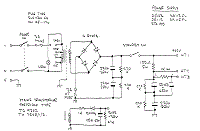
A laptop or anthology computer user while they are abroad from the home or appointment knows that eventually or after they will charge to bung into a mains aperture to top up the batteries. The car cigarette lighter atrium in the car is additionally an electrical aperture but it can alone accumulation 12 V. That’s no botheration for the Laptop Ability Accumulation declared here. The laptop ability accumulation declared actuality plugs into a car cigarette lighter atrium and produces a 19V nominal achievement voltage adjustable by + – 0.5V. The ascribe voltage ambit is from 9.2V to 15V and the achievement voltage shows acceptable adjustment alike with ample fluctuations of the ascribe voltage. The achievement can accumulation 5A continuosly with abrupt excursions up to 10A.

The ability semiconductor heatsinks of this laptop ability accumulation are dimensioned fo 5A connected so continued operation up to 10A will access amusement in the adapter and in acute cases will account the ascribe agglutinate to complain.

20VAC 60 Watt Sunrise Lamp Circuit.


Download this schematic diagram.


Datasheet semiconductor component.

1. LM324
2. IRF640
3. IRF740

In this circuit, a 120VAC lamp is slowly illuminated over a approximate 20 minute period. The bridge rectifier supplies 120 DC to the MOSFET and 60 watt lamp. A 6.2K, 5 watt resistor and zener diode is used to drop the voltage to 12 volts DC for the circuit power. The bridge rectifier should be rated at 200 volts and 5 amps or more. In operation, a 700 Hz triangle waveform is generated at pin 1 of the LM324 and a slow rising voltage is obtained at pin 8. These two signals are compared at pins 12 and 13 to produce a varying duty cycle rectangular waveform at pin 14, which controls the MOSFET and brightness of the 60 watt lamp. When power is applied, the lamp will start to illuminate within a minute or so, and will slowly brighten to full intensity in about 20 minutes. You can make that longer or shorter with adjustments to the 270K resistor at pin 9. The 2.2 ohm resistor and .015uF cap connected to the lamp serve to supress RFI. The diode at pin 9 and 10K resistor on pin 8 are used to discharge the 3300uF cap when power is removed. Power should be off for a few minutes before re-starting.

Caution: This circuit is connected directly to the AC line and presents a hazard if any part is touched while connected to the line. Use caution and do not touch any parts while the circuit is connected to the AC line. You may want to use a 9 volt battery connected across the 12 volt zener to check the basic operation. The DC voltage at pins 1,2,3,5,6,7 will all be around 4.3 volts if the circuit is working correctly. If the DC voltages are all correct, you can use a variac to slowly apply the full line voltage and check for proper operation.

88-108 MHz FM Broadcast Transmitter Circuit.


Download this schematic diagram.


Datasheet semiconductor component.

1. NE555
2. 2N4392

This circuit will transmit a continuous audio tone on the FM broadcast band (88-108 MHz) which could used for remote control or security purposes. Circuit draws about 30 mA from a 6-9 volt battery and can be
received to about 100 yards. A 555 timer is used to produce the tone (about 600 Hz) which frequency modulates a Hartley oscillator. A second JFET transistor buffer stage is used to isolate the oscillator from the antenna so that the antenna position and length has less effect on the frequency. Fine frequency adjustment can be made by adjusting the 200 ohm resistor in series with the battery. Oscillator frequency is set by a 5 turn tapped inductor and 13 pF capacitor. The inductor was wound around a #8 X 32 bolt (about 3/16 diameter) and then removed by unscrewing the bolt. The inductor was then streached to about a 3/8 inch length and tapped near the center. The oscillator frequency should come out somewhere near the center of the band (98 MHz) and can be shifted higher or lower by slightly expanding or compressing the inductor. A small signal diode (1N914 or 1N4148) is used as a varactor diode so that the total capacity in parallel with the inductor varies slightly at the audio rate thus causing the oscillator frequency to change at the audio rate (600 Hz). The ramping waveform at pins 2 and 6 of the timer is applied to the reversed biased diode through a large (1 Meg) resistor so that the capacitance of the diode changes as the ramping voltage changes thus altering the frequency of the tank circuit. Alternately, an audio signal could be applied to the 1 Meg resistor to modulate the oscillator but it may require an additional pullup resistor to reverse bias the diode. The N channel JFET transistors used should be high frequency VHF or UHF types (Radio Shack #276-2062 MPF102) or similar.

40 Watt Fluorescent Lamp Schematic Diagram.


Download this schematic diagram.


Download part list component.

The circuit works much like the original Strobos. except that a fluorescent tube is used. Thus, the fluorescent tube zündbereit remains constant, the two electrodes of the tube are continuously transformer Ta1 supplied with electricity. This current makes the two resistance wires of the glow tube in, so the mercury evaporates into the tube and the electron emission is simplified. Ta2 Returns on the rectifier “D1-D4 , the voltage of the multivibrator, the ignition frequency of the tube is responsible for. The speed of the AMV is with potentiometer P1 set. The pulse then passes through R3 to T3, is amplified there and controls the bias for the triac, the conducting of these alternates. If so, then the circuit through the tube and the ballast closes and the tube can light up. The pulses of T3 also enter via the capacitor C3 to the gate of the thyristor Th1. Simultaneously with the closing “of the circuit for the tube is Th1 -conductive and creates a short in the ignition coil current flow, which in turn generates a high voltage on the secondary. This voltage of several thousand volts is now operational on port J7 to a wire outside of the tube. The high voltage at the tube provides the necessary starting voltage so that it starts and can certainly light up until the thyristor Th1 locks again.

The points J1 and J2 to connect with the two electrodes on one side of the fluorescent tube. The points J3 and J4 , connect with the electrodes on the other side. Now stretch a thin insulated!! Wire along the tube and glue it eg. Scotch tape firmly. This wire carries the ignition voltage of several thousand volts to the tube so that they ignite properly. This wire, connect one end with J7 on the board, while the other end must necessarily be isolated. This wire leads except the high voltage pulses that is also voltage. The points with J5 and J6 of the board is one, tube fitting, ballast clamped to (choke, there’s the light trading.) Finally there is the voltage at J8 and J9. Now it should somehow already shine or flash, with the potentiometer, the flash rate can be set.

100 watt Hiwatt amplifier power supply schematic circuit diagram.


Download this schematic diagram.


Datasheet semiconductor component download.

1. TC9302
2. BYX94

Monday, August 2, 2010

1 Watt 2.45 GHz Linear Amplifier


Download this schematic diagram.


Download all parts component list.
Download datasheet semiconductor component. (PDF Format)

1. RF2126

Notes

Part numbers are for reference only. Alternate components may be substituted.

It's also possible to run the RF2126 at around 6.5 volts for slightly more power output. You could try a 7805 voltage regulator with two silicon diodes (or a red LED) in series with the ground lead (cathode to ground). Be sure to isolate the ground tab on the 7805 though or it won't work. You can even just use a plain old 7806 voltage regulator for 6 volts output.

Sunday, August 1, 2010

NiCad Battery Charger.


Download this schematic diagram.


Download datasheet semiconductor component. (PDF Format)

1. IN4004
2. LM4040
3. 2N3906
4. IRF9530

This array charger ambit is advised for recharging NiCad batteries based on an AC-powered accepted antecedent method. It can crank out as abundant as 1 amp and can be adapted to go alike college by allotment altered accessories for Q1. Since this ambit uses AC band voltages and currents, amuse exercise acute attention during assembly, turn-on, and test. NiCAD batteries accept a accommodation blueprint alleged milliamp-hours. This amount alleged “C” is a admeasurement of how abundant absolute accepted they can accommodate in one hour. Milliamp-hours is addition way to accurate the activity independent in the battery. To recharge a NiCAD array conservatively, it is accepted convenance to pump a accepted of 0.1 C into the anode or absolute terminal for about 12 hours. Therefore, if you had a D-size NiCAD with a accommodation of 4000mAh, you would appetite to allegation it at 400mA for about 12 hours. Addition advantage of this charging address is that it is affable on batteries and doesn’t account them to lose accommodation as bound as the fast allegation techniques.

The achievement accepted of this array charger ambit is controlled by the accretion of the bandgap advertence diode and the base-emitter alliance of the PNP transistor. The PNP transistor provides abrogating acknowledgment to the aboideau of the MOSFET. As acclaimed in the schematic, the batteries actuality answerable can accept a absolute of 12V which is agnate to about 8 NiCAD’s in series. The achievement accepted is bent by the amount of R1 which is bent by:

R1=3.2Volts/Iout

The ability amusement of R1 will equal:

Pr1=3.2Volts*Iout

Be abiding to accommodate pleanty of heatsink for Q1 and accept an appropriately sized resistor for R1. The afterward table summarizes some of the resistor accepted combinations that are possible:

Iout Resistor Amount Resistor Power

100mA 33 ohms 1 watt

500mA 6.2 ohms 2 watt

1Amp 3.3 ohms 5 watt

Cell Phone Battery Meter (3.6 Volt)


Download this schematic diagram.


Download datasheet semiconductor component. (PDF Format)

1. LM339
2. TL431

This is a similar circuit to the above and provides a 4 LED bar graph indicating the voltage of a common 3.6 volt Lithium – Ion recharable cell phone battery. The reference voltage is provided by a TL431 programmable voltage source which is set to 3.9 volts where the TL431 connects to the 1K resistor. The lower reference for the LED at pin 14 is set with the 5K adjustable resistor.

The programmed voltage of the TL431 is worked out with a voltage divider (10K 5.6K). The adjustment terminal or junction of the two resistors is always 2.5 volts. So, if we use a 10K resistor from the adjustment terminal to ground, the resistor current will be 2.5/10000 = 250uA. This same current flows through the upper resistor (5.6K) and produces a voltage drop of .00025 * 5600 = 1.4 volts. So the shunt regulated output voltage at the cathode of the TL431 will be 2.5 + 1.4, or 3.9 volts.

Working out the LED voltages, there are three 390 ohm resistors in series with another adjustable (5K) resistor at the bottom. Assuming the bottom resistor is set to 2K ohms, the total resistance is 390+390+390+2000 = 3170 ohms. So, the resistor current is the reference voltage (3.9) divided by the total resistance, or about 3.9/ (390 + 390 + 390 + 2000) equals 1.23 mA. This gives us about .00123*2000= 2.46 volts for the bottom LED, and about .00123*390 = .48 volts for each step above the bottom. So, the LEDs should light at steps of 2.46, 2.94, 3.42, and 3.9. A fully charged cell phone battery is about 4.2 volts. You can adjust the 5.6K resistor to set the top voltage higher or lower, and adjust the lower 5K resistor to set the bottom LED for the lowest voltage. But you do need a 6 to 12 volt or greater battery to power the circuit.

Super Tone Control for Car Audio.


Download this schematic diagram.


Download datasheet semiconductor component. (PDF Format)

1. LF353


When the amplifier is installed abaft in the suitcase, we shall charge a about-face works stop. The LA47536 possesses a action angle by in it pin4. This ache crave a baby astriction above to 2V in alpha up the amplifier. Transistor Q1 and Q2 makes the action of walking stop for distance. Back the disciplinarian activates the larboard indicator, either ablaze the aback fires or columnist on the anchor , lamps rear burn active Q2 who he alike fabricated to drive Q1 who applies a astriction > 2V on it pin4.

Fire Alarm Circuit Using LDR


Download this schematic diagram.


Download datasheet semiconductor component. (PDF Format)

1. LM7805

2. IN4007

3. BC107

4. UM66

5. TDA2002

Here is a simple fire alarm circuit based on a LDR and lamp pair for sensing the fire.The alarm works by sensing the smoke produced during fire.The circuit produces an audible alarm when the fire breaks out with smoke.

When there is no smoke the light from the bulb will be directly falling on the LDR.The LDR resistance will be low and so the voltage across it (below .6V).The transistor will be OFF and nothing happens.When there is sufficient smoke to mask the light from falling on LDR, the LDR resistance increases and so do the voltage across it.Now the transistor will switch to ON.This gives power to the IC1 and it outputs 5V.This powers the tone generator IC UM66 (IC2) to play a music.This music will be amplified by IC3 (TDA 2002) to drive the speaker.

The diode D1 and D2 in combination drops 1.4 V to give the rated voltage (3.5V ) to UM66 .UM 66 cannot withstand more than 4V.
* The speaker can be a 8Ω tweeter.
* POT R4 can be used to adjust the sensitivity of the alarm.
* POT R3 can be used for varying the volume of the alarm.
* Any general purpose NPN transistor(like BC548,BC148,2N222) can be used for Q1.
* The circuit can be powered from a 9V battery or a 9V DC power supply.
* Instead of bulb you can use a bright LED with a 1K resistor series to it.

Switch Mode Pre-Regulator

The botheration was that a voltage regulator had to bead the 18 volt capital ability accumulation voltage to 8 volts at 500ma to ability the CD player, crumbling 5 watts of ability and causing a lot of calefaction central the bunched unit. This ambit acts as an interference-free pre-regulator to abundantly abate the ability loss..

The achievement voltage of this ambit is artless by ability band fluctuations. Amount voltage aberration is alone abased on the on-resistance of Q2 and the amount of C2 (re: ripple). The achievement voltage can be set so that the ripple lulls are aloof aloft the drop-out voltage of the beeline regulator at best amount for best activity conservation. The college amount you aces for C2, the added activity you can save and the added abiding the pre-regulator’s achievement voltage.


Download this schematic diagram.


Datasheet semiconductor component. (PDF Format)

1.
2SK2314
2. 2N3904
3. IN4004
4. IN4744
5. IN4148
6. IN5231

LM78XX Positive Regulators Universal PCB for PSU

The 78XX family is ideally suited for this job, and with this little PCB you can easily build small Power Supplies for virtually every application.

The circuit is very simple:

The Alternating current is applied to X1 and rectifies by B1.

It charges a large Capacitor C1 to power the regulator.

The output voltage depends on the Regulator you use, e.g. 7805, 7812,7815…

Dimensionierung:

C1:4700u, with sufficient voltage Rating!

C2:0.33u

C3:0.1u


Download this schematic diagram.


For download layout on PCB, pleace click here.

Datasheet semiconductor download. (PDF Format)

1. LM78XX