Dengan mengikuti program PTC (Paid To Click) kita bisa mendapatkan penghasilan tambahan dari internet dengan mengklik iklan-iklan yang disediakan oleh admin, tentunya tanpa biaya sepeserpun alias geratis. Tapi bagi anda sebagai pemula dalam hal ini, perlu diketahui tidak semua program PTC yang ada diinternet membayar kita, sebagaian mereka hanya scam. Jadi kita harus benar-benar teliti dan hati-hati dalam memilih program PTC mana yang dapat kita percaya dan dapat kita ikuti.
Jika anda ingin mengikuti program PTC, silahkan anda klik
DISINI
dan link tadi akan membawa anda keblog saya dimana disana telah saja jelaskan apa dan bagaimana cara mengikuti program PTC, termasuk saya juga saya berikan rekomendasi PTC terpercaya bila anda ingin mengikuti program tersebut.
Wednesday, September 2, 2009
Monday, July 6, 2009
25 Watt MosFet Audio Amplifier

Click here for download this schematic
Parts:
R1,R4_________47K 1/4W ResistorsR2____________4K7 1/4W Resistor
R3____________1K5 1/4W Resistor
R5__________390R 1/4W Resistor
R6__________470R 1/4W Resistor
R7___________33K 1/4W Resistor
R8__________150K 1/4W Resistor
R9___________15K 1/4W Resistor
R10__________27R 1/4W Resistor
R11_________500R 1/2W Trimmer Cermet
R12,R13,R16__10R 1/4W Resistors
R14,R15_____220R 1/4W Resistors
R17___________8R2 2W Resistor
R18____________R22 4W Resistor (wirewound)
C1___________470nF 63V Polyester Capacitor
C2___________330pF 63V Polystyrene Capacitor
C3,C5________470µF 63V Electrolytic Capacitors
C4,C6,C8,C11_100nF 63V Polyester Capacitors
C7___________100µF 25V Electrolytic Capacitor
C9____________10pF 63V Polystyrene Capacitor
C10____________1µF 63V Polyester Capacitor
Q1-Q5______BC560C 45V 100mA Low noise High gain PNP Transistors
Q6_________BD140 80V 1.5A PNP Transistor
Q7_________BD139 80V 1.5A NPN Transistor
Q8_________IRF530 100V 14A N-Channel Hexfet Transistor
Q9_________IRF9530 100V 12A P-Channel Hexfet Transistor
semiconductor list componen datasheet (PDF Format)
1. BC.560C
2. BD.140
3. BD.139
4. IRF.530
5. IRF.9530
6 Input Mixer

A simple mixer with 3 line inputs and 3 mic inputs using commonly available parts.
click here for download this schematic diagram
The mixer circuit above has 3 line inputs and 3 mic inputs. The mic inputs are suitable for low impedance 200-1000R dynamic microphones. An ECM or condenser mic can also be used, but must have bias applied via a series resistor. As with any mixer circuit, a slight loss is always introduced. The final summing amplifier has a gain of 2 or 6dB to overcome this. The Input line level should be around 200mV RMS.
The mic inputs are amplified about 100 times or 40dB, the total gain of the mixer including the summing amplifier is 46dB. The mic input is designed for microphones with outputs of about 2mV RMS at 1 meter. Most dynamic microphones meet this standard.
The choice of op-amp is not critical in this circuit. Bipolar, FET input or MOS type op-amps can therefore be used; i.e 741, LF351, TL061, TL071, CA3140 etc. The power supply is a dual positive and negative supply, two 9 Volt batteries may be used as shown above or a power supply is recommended for longer periods of use.
Download list datasheet semiconductor component. (PDF Format)
1. LM741
2. LM324
3. LF351
4. NE5534
5. TL071
High Quality Intercom

click here for download this schematic diagarm
This circuit consists of two identical intercom units. Each unit contains a power supply, microphone preamplifier, audio amplifier and a Push To Talk (PTT) relay circuit. Only 2 wires are required to connect the units together. Due to the low output impedance of the mic preamp, screened cable is not necessary and ordinary 2 core speaker cable, or bell wire may be used.
The schematic can be broken into 34 parts, power supply, mic preamp, audio amplifierand PTT circuit. The power supply is designed to be left on all the time, which is why no on / off switch is provided. A standard 12 V RMS secondary transformer of 12VA will power the unit. Fuses are provided at the primary input and also secondary, before the rectifier. The 1 A fuse needs to be a slow blow type as it has to handle the peak rectifier current as the power supply electrolytics charge from zero volts.
The microphone amplifier is a 2 transistor direct coupled amplifier. BC108B transistors will work equally well in place of the BC109C transistors. The microphone used is a 3 terminal electret condenser microphone insert. These are popular and require a small current to operate. The preamp is shown in my audio circuit section as well, but has a very high gain and low distortion. The last transistor is biased to around half the supply voltage; this provides the maximum overload margin for loud signals or loud voices. The gain may be adjusted with the 10k preset. Sensitivity is very high, and a ticking clock can easily be heard from the distant loudspeaker.
The amplifier is based on the popular National Semiconductor LM380. A 50 mV input is all thats required to deliver 2W RMS into an 8 ohm loudspeaker. The choice of loudspeaker determines overall sound quality. A small loudspeaker may not produce a lot of bass, I used an old 8 inch radio loudspeaker. The 4.7u capacitor at pin 1 of the LM380 helps filter out any mains hum on the power supply. This can be increased to a 10u capacitor for better power supply rejection ratio.
The push to talk (PTT) circuit is very simple. A SPDT relay is used to switch between mic preamplifier output or loudspeaker input. The normally closed contact is set so that each intercom unit is "listening". The non latching push button switch must be held to talk. The 100u capacitor across the relay has two functions. It prevents the relays back emf from destroying the semiconductors, and also delays the release of the relay. This delay is deliberate, and prevents any last word from being "chopped" off.
Download datasheet semiconductor component. (PDF Format)
1. BC.109C
2. LM.380
3. IN.4001
Micro Power AM Broadcast Transmitter
download this schematic diagram
download semiconductor list datasheet:
1. 2N3904
2. 74HC14
In this circuit, a 74HC14 hex Schmitt trigger inverter is used as a square wave oscillator to drive a small signal transistor in a class C amplifier configuration. The oscillator frequency can be either fixed by a crystal or made adjustable (VFO) with a capacitor/resistor combination. A 100pF capacitor is used in place of the crystal for VFO operation. Amplitude modulation is accomplished with a second transistor that controls the DC voltage to the output stage. The modulator stage is biased so that half the supply voltage or 6 volts is applied to the output stage with no modulation. The output stage is tuned and matched to the antenna with a standard variable 30-365 pF capacitor. Approximately 20 milliamps of current will flow in the antenna lead (at frequencies near the top of the band) when the output stage is optimally tuned to the oscillator frequency. A small 'grain of wheat' lamp is used to indicate antenna current and optimum settings. The 140 uH inductor was made using a 2 inch length of 7/8 inch (OD) PVC pipe wound with 120 turns of #28 copper wire. Best performance is obtained near the high end of the broadcast band (1.6 MHz) since the antenna length is only a very small fraction of a wavelength. Input power to the amplifier is less than 100 milliwatts and antenna length is 3 meters or less which complies with FCC rules. Output power is somewhere in the 40 microwatt range and the signal can be heard approximately 80 feet. Radiated power output can be approximated by working out the antenna radiation resistance and multiplying by the antenna current squared. The radiation resistance for a dipole antenna less than 1/4 wavelength is
R = 80*[(pi)^2]*[(Length/wavelength)^2]*(a factor depending on the form of the current distribution) The factor depending on the current distribution turns out to be [(average current along the rod)/(feed current)]^2 for short rods, which is 1/4 for a linearly-tapered current distribution falling to zero at the ends. Even if the rods are capped with plates, this factor cannot be larger than 1. Substituting values for a 9.8 foot dipole at a frequency of 1.6 MHz we get R= 790*.000354*.25 = .07 Ohms. And the resistance will be only half as much for a monopole or 0.035 Ohms. Radiated power at 20 milliamps works out to about I^2 * R = 14 microwatts.
AM DSB TRANSMITTER FOR HAMS
download list datasheet semiconductor component. (PDF Format)
1. IN.4148
2. BC.548
3. 2N.2222A
4. SL.100B
The circuit of AM transmitter is designed to transmit (amplitude modulated) DSB (double side band) signals. A modulated AM signal consists of a carrier and two symetrically spaced side bands. The two side bands have the same amplitude and carry the same information. In fact, the carrier itself coveys or carries no information. In a 100% modulated AM signal 2/3 rd of the power is wasted in the carrier and only 1/6th of the power is contained in each side band.
In this transmitter we remove the carrier and transmitt only the two side bands. The effective output of the circuit is three times that of an equivalent AM transmitter.
Op Amp IC741 is used here as a microphone amplifier to amplify the voice picked up by the condenser microphone. The output of the op amp is fed to the double balanced modulator (DBM) build around four IN4148 diodes. The modulation level can be adjusted with the help of preset VR1.
The carrier is generated using crystal oscillator wired around BC548 transistor T2. The carrier is further amplified by transistor T1, which also acts as a buffer between carrier oscillator and the balanced modulator. The working frequency of the transmitter can be changed by using crystals of different frequencies. For multi frequency operation, selection of different crystals can be made using a selector switch.
Ths output of the DBM contains only the product (of audio and carrier) frequencies. The DBM suppresses both the input signals and produces double side band suppressed carrier (DSBSC) at its output. However, since the diodes used in the balanced modulator are not fully matched, the output of the DBM does contain some residual carrier. This is known as carrier leakage. By adjusting the 100 ohm preset VR2 and trimmer C7 you can null the carrier leakage.
To receive DSB signals you need a beat frequency oscillator to reinsert the missing carrier. If you don't have a beat frequency oscillator, or want to transmitt only AM signal, adjust preset VR2 to leak some carrier so that you can receive the signals on any ordinary radio receiver. In AM mode 100% modulation can be attained by adjusting preset VR1 and VR2.
The DSBSC signal available at the output of the balanced modulator is amplified by two stages of RF linear amplifiers. Transistor 2N2222A (T3) is used as an RF pre amplifier, which provides enough signal amplification to drive the final power amplifier build around transistor SL100B. The output of the final power amplifier is connected to the antenna.
All coils are to be wound ferrite balun core (same as used in TV balun transformer of size 1.4 cm * 0.6 cm) using 24 swg enameled copper wire. Proper heat sink should be provided for SL100B transistor used as final power amplifier.
X1 - 8+8 Turns Bifalar 24 SWG On TV Balune Core
X2 - Primary 12 Turns, Secondary 4 Turns. 24 SWG on TV Balun Core (dot indicates start of coil).
X3 - 20 Turns 24 SWG on TV Balun Core
Range of the circuit depends on the type of antenna used. It is very important to use matched antenna to radiate the signals effectively. I used horizontal dipole antenna, which is simple and easy to construct. For 7 MHz, ie 40 meter ham band the length of dipole antenna will be 20 meter. Use 75 Ohms co-axial cable to connect antenna and transmitter. I was able to get 57 report from station 80 kilometer away. You can easily add a Linear RF amplifier using IRF830 to get more power.
Circuit designed by YUJIN BOBY VU3PRX
Published in Electronics For You Dec 2000
Sunday, May 31, 2009
5,000W ultra-light, high-power amplifier, without switching-mode power supply

Download this schematic diagram.
download semiconductor component datasheet. (PDF Format)
1. MPSA.42
2. MPSA.92
3. MPSW.42
4. MPSW.92
5. 2SA1302
6. 2SC3281
7. MJL21193
8.MJL21194
9. LM7815
10. LM7915
This circuit is of an 2x 2,500W RMS stereo amplifier, super-light and without switching-mode power supply. The circuit just shows a channel, and the power supply that it assists to the two channels. The audio circuit should be duplicated, but the power supply assists to the two channels without problems.
A special care should be destined to the insulating transformer of the audio line, that should be of audio-high-quality, of the type used in microphone pre amps input line. The whole group (2 channels) of 5,000W RMS it should not weigh more than 32 lbs, already inside of an appropriate metallic box.
WARNING:
This circuit is exclusively for amateur use. It contains not-isolated parts of the electric AC net and it can be very dangerous. The connections for the speakers are not isolated of the domestic AC net and it requests extra care. This procedure seeks to substitute a conventional power supply with great weight and cost reduction, without necessarily to use a switching-mode power supply.
This procedure cannot be allowed in some countries for commercial-use. The author doesn't have any responsibility for the form as that circuit it will be applied.
Wednesday, May 20, 2009
LM2577 5V to 12V DC Converter step up Voltage Regulator
DC to DC step up voltage regulator. Wide input voltage 3.5Vdc to 40Vdc. This is Circuit DC to DC converter step up vol

Download this schematic.
Download list semiconductor datasheet. (PDF Format)
1. LM2577
2. IN5821
http://www.circuits-lab.com/

Download this schematic.
Download list semiconductor datasheet. (PDF Format)
1. LM2577
2. IN5821
http://www.circuits-lab.com/
Injector Pulse Width Monitor with LM324 ,LM3914
The schematic for the pulse width monitor. The heart of the circuit is the transistor current source which charges cap C10 to form an integrator. The theory is that the cap is charged and the voltage across it increases linearly for the amount of time that the injector is energized. As the injector is switched off the voltage in C10 is stored in cap C9 and then C10 is reset to 0 volts to get ready for the next cycle. The output of the circuit is the voltage across cap C9, this voltage is fed directly into U3 the bar graph chip to be displayed as a value between 1-10 on the LEDs. Potentiometer R31 sets the charge rate on C10 and basically sets the max injector on time that can be displayed.

Download this schematic diagaram.
download datasheet the semiconductor component. (PDF Format)
1. LM324
2. LM3914
3. CD4058
4. LM7805
5. MN3206
6. MN3906
7. 2N2222
8. IN214
9. IN5233
Injector Pulse Width Monitor with LM324 ,LM3914 - [Link]
Temperature Monitor with IC LM741 or LM301
Using a thermistor in the position shown makes a heat activated sensor. A change in temperature will alter the output of the opamp and energize the relay and light the LED. Swapping the position of the thermistor and 47k resistor makes a cold or frost alarm.

Download semiconductor parts datasheet. (PDF Format)
1. LM741
2. LM301
3. BC182B
Temperature Monitor with IC LM741 or LM301 - [Link]
2N3055 Simple inverter 5W
This simple inverter. The main aim of this circuit is to provide a suitable supply for all kind of low power battery chargers that normally connect to the mains such as mobile phones, electric shavers, etc, even an electronic neon light rated at 5W was successfully connected. Only easily obtainable components are used.

Download this schematic diagram.
Download list datasheet semiconductor parts. (PDF Format)
1. 2N3055
http://www.circuits-lab.com/

Download this schematic diagram.
Download list datasheet semiconductor parts. (PDF Format)
1. 2N3055
http://www.circuits-lab.com/
Nagative voltage generation using 555 timer
This 555 timer based PWM controller features almost 0..100% pulse width regulation using R1, while keeping the oscillator frequency relatively stable. The frequency is dependent on values of R1 and C1, values shown will give a frequency range from about 170 to 200 Hz. Any 555 chip will do, CMOS is fine as well. Diodes are not critical, I used 1N4148. Total cost of parts is about $2. As the whole thing is quite trivial, it’s very easy to build on prototyping board like I did.

Download this schematic diagram.
Download semiconductor datasheet parts. (PDF Format)
1. NE555
2. BD140
PWM Speed Motor Controller By IC 555-Electronic control circuit - [Link]
Power Amplifier with STK40xx Series Module
The series STK40xx is power amplifiers in completed form in a nutshell. They are characterized by the very good quality of sound and their low price. It is easy we make a power amplifier using only few external components. The STKxxxx amplifiers, for them we will find in enough eponymous stereo amplifiers , but also in enough activety loudspeakers. They do not need a lot of special knowledge of manufacture, only that attention in pins, in order to they do not break, and one good power supply. Details for the various types of series, voltage of work and the output power, see the Table A

Download this schematic diagram.
Download datasheet semiconductor component. (PDF Format)
1. STK 40XX
Power Amplifier with STK40xx Series Module - [Link]
LM317T Voltage Regulator with Pass Transistor
The LM317T output current can be increased by using an additional power transistor to share a portion of the total current. The amount of current sharing is established with a resistor placed in series with the 317 input and a resistor placed in series with the emitter of the pass transistor.

Download this schematic.
Download list datasheet semiconductor parts. (PDF Format)
1. 2N2955
2. LM317A
3. IN4002
http://www.circuits-lab.com/

Download this schematic.
Download list datasheet semiconductor parts. (PDF Format)
1. 2N2955
2. LM317A
3. IN4002
http://www.circuits-lab.com/
Wednesday, May 6, 2009
Line Driver
Description:
A stereo line driver for feeding long cables or buffering an audio source.
Download this schematic diagram.
Download semiconductor parts datasheet. (PDF Format)
1. BC109C
Notes
This preamplifier has a low output impedance, and is designed to drive long cables, allowing you to listen to a remote music source without having to buy expensive screened cables. The very low output impedance of around 16 ohms at 1KHz, makes it possible to use ordinary bell wire,loudspeaker or alarm cable for connection. The preamplifier must be placed near the remote music source, for example a CD player. The cable is then run to a remote location where you want to listen. The output of this preamp has a gain of slightly less than one, so an external amplifier must be used to drive loudspeakers.
Buffer Amplifier
Description:
A hifi preamplifier designed to convert high output impedance amplifiers to 600 ohm outputs.
Download this schematic diagram.

Download this image.
List datasheet semiconductor parts. (PDF Format)
1. BC547C
2. BC557C
3. 2SA1358
4. 2SC3421
TDA2030 8w Amplifier

Download this schematic diagram.
Download list datasheet semiconductor parts. (PDF Format)
1. TDA2030
2. IN4001
Notes
Monday, April 20, 2009
12 Volt 30 Amp Power Supply

Download this schematic diagram.
Download list datasheet semiconductor parts. (PDF Format)
1. TIP2955
2. LM7812
Description
Using a single 7812 IC voltage regulator and multiple outboard pass transistors, this power supply can deliver output load currents of up to 30 amps. The design is shown below:The input transformer is likely to be the most expensive part of the entire project. As an alternative, a couple of 12 Volt car batteries could be used. The input voltage to the regulator must be at least several volts higher than the output voltage (12V) so that the regulator can maintain its output. If a transformer is used, then the rectifier diodes must be capable of passing a very high peak forward current, typically 100amps or more. The 7812 IC will only pass 1 amp or less of the output current, the remainder being supplied by the outboard pass transistors. As the circuit is designed to handle loads of up to 30 amps, then six TIP2955 are wired in parallel to meet this demand. The dissipation in each power transistor is one sixth of the total load, but adequate heat sinking is still required. Maximum load current will generate maximum dissipation, so a very large heat sink is required. In considering a heat sink, it may be a good idea to look for either a fan or water cooled heat sink. In the event that the power transistors should fail, then the regulator would have to supply full load current and would fail with catastrophic results. A 1 amp fuse in the regulators output prevents a safeguard. The 400mohm load is for test purposes only and should not be included in the final circuit.
for detail, pleace click here
0 - 300V Adjustable Power Supply.

Download this schematic.
Download datasheet semiconductor parts. (PDF Format)
1. BUZ326
2. BC547
Introduction
To prevent my high voltage experiments to go up in smoke completely, I designed
a simple circuit which can provide an adjustable voltage source of 0 to 330 Volt..
The supply is short-ciruit proof: the current is limited to about 100mA.
Circuit description
TR1 is a 1:1 mains transformer; it is included for safety.
The mains voltage from TR1 is rectified with bridge D1 (1Amp / 500V) and large elcap C1.
T1 is switched as a source follower: the source of T1 will follow the voltage of the
wiper of R3. D2 is included to protect the gate of T1; although in theory not necessary
I strongly recommend to include it!
T2 and shunt resistor R2 build the current limiter. When the output current becomes too high, T2 will discharge
the gate of T1. This will prevent the current to become too high.
The value of R3 has been determined experimentally; it depends also on the Hfe of T2 so you may need to tune the value of R2.
Note that T1 needs a large heatsink: in worst case T1 will dissipate 330V x 100mA = 33Watt!
Instead of a BUZ 326 (400V/10.5Amp) you can also use an IRF740 (400V/10Amp).
The output impedance of the power supply is determined by the beta of T1, so the larger the MOSFET
the lower the output impedance!
Monday, April 13, 2009
15 Watt Mini Amplifier
A 15 watt amplifier made using discrete components. Sergio designed this circuit for his Electronics Level II course.

Download this schematic diagram.
Download list datasheet semiconductor component. (PDF Format)
1. 2N3904
2. 2N2907A
3. 2N3906
4. IN4002
Notes:
This amplifier uses a dual 20 Volt power supply and delivers 15 watts RMS into an 8 ohm load. Q1 operates in common emitter, the input signal being passed to the bias chain consisting of Q8, Q9, D6, D13 and D14. Q8 and Q9 provide a constant current through the bias chain to minimize distortion, the output stage formed by a discrete darlington pair (Q2,Q4) and (Q7,Q11). The last two transistors are power Transitors, specifically the 2N3055 and MJ2955. The 7.02K resistor, R16 was made using a series combination of a 4.7K, 680 Ohms, and two 820 Ohms. The 1.1K resistor, R3 was made using a 100 Ohms and a 1K resistor. You can use this circuit with any walkman or CD player since it is designed to take a standard 500mv RMS signal.
http://www.zen22142.zen.co.uk/
100W Guitar Power Amplifier
The power amp board has remained unchanged since it was first published in 2002. It certainly isn't broken, so there's no reason to fix it. The photo below shows a fully assembled board (available as shown as M27). Using TIP35/36C transistors, the output stage is deliberately massive overkill. This ensures reliability under the most arduous stage conditions. No amplifier can be made immune from everything, but this does come close.


The power amp (like the previous version) is loosely based on the 60 Watt amp previously published (Project 03), but it has increased gain to match the preamp. Other modifications include the short circuit protection - the two little groups of components next to the bias diodes (D2 and D3). This new version is not massively different from the original, but has adjustable bias, and is designed to provide a "constant current" (i.e. high impedance) output to the speakers - this is achieved using R23 and R26. Note that with this arrangement, the gain will change depending on the load impedance, with lower impedances giving lower power amp gain. This is not a problem, so may safely be ignored.
Should the output be shorted, the constant current output characteristic will provide an initial level of protection, but is not completely foolproof. The short circuit protection will limit the output current to a relatively safe level, but a sustained short will cause the output transistors to fail if the amp is driven hard. The protection is designed not to operate under normal conditions, but will limit the peak output current to about 8.5 Amps. Under these conditions, the internal fuses (or the output transistors) will probably blow if the short is not detected in time.

Download this schematic diagram.
Download datasheet semiconductor component. (PDF Format)
1. BC559
2. BC549
3. BD139
4. BD140
5. TIP35C
6. TIP36C
Guitar Pre-Amplifier
A photo of the Revision-A preamp is shown below. You'll see that there are two dual opamps, but the schematic only shows one. This is the main part of the Rev-A update - the output section now has gain (which is easily selected), and a better buffered low output impedance. The remainder of the circuit is unchanged. Full details of the new version are available on the secure site for those who purchase the PCBs.

Download this image.

Download this schematic diagram.
semiconductor datasheet component. (PDF Format)
1. TL072
2. BC549

Download this image.
The preamp circuit is shown in Figure 1, and has a few interesting characteristics that separate it from the "normal" - assuming that there is such a thing. This is simple but elegant design, that provides excellent tonal range. The gain structure is designed to provide a huge amount of gain, which is ideal for those guitarists who like to get that fully distorted "fat" sound.
However, with a couple of simple changes, the preamp can be tamed to suit just about any style of playing. Likewise, the tone controls as shown have sufficient range to cover almost anything from an electrified violin to a bass guitar - The response can be limited if you wish (by experimenting with the tone control capacitor values), but I suggest that you try it "as is" before making any changes.
Download this schematic diagram.
semiconductor datasheet component. (PDF Format)
1. TL072
2. BC549
Automatic Loudness Control

In order to obtain a good audio reproduction at different listening levels, a different tone-controls setting should be necessary to suit the well known behaviour of the human ear. In fact, the human ear sensitivity varies in a non-linear manner through the entire audible frequency band, as shown by Fletcher-Munson curves.
A simple approach to this problem can be done inserting a circuit in the preamplifier stage, capable of varying automatically the frequency response of the entire audio chain in respect to the position of the control knob, in order to keep ideal listening conditions under different listening levels.
Fortunately, the human ear is not too critical, so a rather simple circuit can provide a satisfactory performance through a 40dB range.
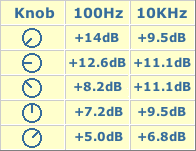
The circuit is shown with SW1 in the "Control-flat" position, i.e. without the Automatic Loudness Control. In this position the circuit acts as a linear preamplifier stage, with the voltage gain set by means of Trimmer R7.
Switching SW1 in the opposite position the circuit becomes an Automatic Loudness Control and its frequency response varies in respect to the position of the control knob by the amount shown in the table below.
C1 boosts the low frequencies and C4 boosts the higher ones. Maximum boost at low frequencies is limited by R2; R5 do the same at high frequencies.
Technical data:
Frequency response referred to 1KHz and different control knob positions:
Total harmonic distortion at all frequencies and 1V RMS output: <0.01%
Notes:
- SW1 is shown in "Control flat" position.
- Schematic shows left channel only, therefore for stereo operation all parts must be doubled except IC1, C6 and C8.
- Numbers in parentheses show IC1 right channel pin connections.
- R7 should be set to obtain maximum undistorted output power from the amplifier with a standard music programme source and P1 rotated fully clockwise.
9v Battery Voltage Monitor using a LTC1440 Comparator
This circuit turns on a LED whenever the voltage of a standard 9v battery connected to the circuit drops below 7.2 volts. It uses a LTC1440 comparator, which also contains a 1.18v reference diode. In standby mode, the circuit draws only 4uA.


Battery Monitor Circuits
Master Schematic Category List - David A. Johnson, P.E.
Friday, April 10, 2009
120 VAC Lamp Dimmer
The full wave phase control circuit below was found in a RCA power circuits book from 1969. The load is placed in series with the AC line and the four diodes provide a full wave rectified voltage to the anode of a SCR. Two small signal transistors are connected in a switch configuration so that when the voltage on the 2.2uF capacitor reaches about 8 volts, the transistors will switch on and discharge the capacitor through the SCR gate causing it to begin conducting. The time delay from the beginning of each half cycle to the point where the SCR switches on is controlled by the 50K resistor which adjusts the time required for the 2uF capacitor to charge to 8 volts. As the resistance is reduced, the time is reduced and the SCR will conduct earlier during each half cycle which applies a greater average voltage across the load. With the resistance set to minimum the SCR will trigger when the voltage rises to about 40 volts or 15 degrees into the cycle. To compensate for component tollerances, the 15K resistor can be adjusted slightly so that the output voltage is near zero when the 50K pot is set to maximum. Increasing the 15K resistor will reduce the setting of the 50K pot for minimum output and visa versa. Be careful not to touch the circuit while it is connected to the AC line.

visit: http://www.discovercircuits.com/list.htm

visit: http://www.discovercircuits.com/list.htm
Variable Voltage and Current Power Supply

Download this schematic.
Download list datasheet semiconductor parts. (PDF Format)
1. 2N3055
2. LM1458
Another method of using opamps to regulate a power supply is shown below. The power transformer requires an additional winding to supply the op-amps with a bipolar voltage (+/- 8 volts), and the negative voltage is also used to generate a reference voltage below ground so that the output voltage can be adjusted all the way down to 0. Current limiting is accomplished by sensing the voltage drop across a small resistor placed in series with the negative supply line. As the current increases, the voltage at the wiper of the 500 ohm pot rises until it becomes equal or slightly more positive than the voltage at the (+) input of the opamp. The opamp output then moves negative and reduces the voltage at the base of the 2N3053 transistor which in turn reduces the current to the 2N3055 pass transistor so that the current stays at a constant level even if the supply is shorted. Current limiting range is about 0 - 3 amps with components shown. The TIP32 and 2N3055 pass transistors should be mounted on suitable heat sinks and the 0.2 ohm current sensing resistor should be rated at 2 watts or more. The heat produced by the pass transistor will be the product of the difference in voltage between the input and output, and the load current. So, for example if the input voltage (at the collector of the pass transistor) is 25 and the output is adjusted for 6 volts and the load is drawing 1 amp, the heat dissipated by the pass transistor would be (25-6) * 1 = 19 watts. In the circuit below, the switch could be set to the 18 volt position to reduce the heat generated to about 12 watts.
http://www.discovercircuits.com/list.htm
Variable 3 - 24 Volt / 3 Amp Power Supply
This regulated power supply can be adjusted from 3 to 25 volts and is current limited to 2 amps as shown, but may be increased to 3 amps or more by selecting a smaller current sense resistor (0.3 ohm). The 2N3055 and 2N3053 transistors should be mounted on suitable heat sinks and the current sense resistor should be rated at 3 watts or more. Voltage regulation is controlled by 1/2 of a 1558 or 1458 op-amp. The 1458 may be substituted in the circuit below, but it is recommended the supply voltage to pin 8 be limited to 30 VDC, which can be accomplished by adding a 6.2 volt zener or 5.1 K resistor in series with pin 8. The maximum DC supply voltage for the 1458 and 1558 is 36 and 44 respectively. The power transformer should be capable of the desired current while maintaining an input voltage at least 4 volts higher than the desired output, but not exceeding the maximum supply voltage of the op-amp under minimal load conditions. The power transformer shown is a center tapped 25.2 volt AC / 2 amp unit that will provide regulated outputs of 24 volts at 0.7 amps, 15 volts at 2 amps, or 6 volts at 3 amps. The 3 amp output is obtained using the center tap of the transformer with the switch in the 18 volt position. All components should be available at Radio Shack with the exception of the 1558 op-amp.

Download this schematic.
Download datasheet semiconductor component. (PDF Format)
1. 2N3055
2. 2N3053
3. 2N3904
4. LM1558

Download this schematic.
Download datasheet semiconductor component. (PDF Format)
1. 2N3055
2. 2N3053
3. 2N3904
4. LM1558
Sunday, April 5, 2009
0-30V Stabilized Variable Power Supply with Current Control

This is high quality stabilized power supply circuit diagram. You will able to adjust the output voltage from 0 volt up to 30 volt DC. You also able to adjust the current output value from 0.002 A to 3 A.
Detail explanation include the PCB layout, visit this page
Flashing Heart Circuit
This is LED flashing circuit, the circuit is quite simple. Alternatively, you could be create another shape, not just heart shape.

Component list:
| Resistors | ||
| R1, R2 | - | 470 ohm, 1/2-watt |
| R3-R5 | - | 100 ohm, 3-watt |
| R6-R8 | - | 1000 ohm, 1.4-watt |
| R9 | - | 5000 ohm potentiometer |
| Capacitors | ||
| C1, C2 | - | 100uF, 16 volts, electrolytic radial |
| Semiconductors | ||
| IC1 | - | 4047, low power monostable/astable multivibrator |
| Q1-Q3 | - | 2n3643 NPN transistor or equivalent |
Download datasheet semiconductor component: 1. 4047 2. 2N3643 | ||
| Diodes | ||
| LED1-LED84 | - | yellow light-emitting diode |
| LED85-LED126 | - | red light-emitting diode |
| LED127-LED142 | - | green light-emitting diode |
| Other components | ||
| PS1 | - | 12VDC @ 500mA wall transformer |
| Miscellaneous: Jumper wire, solder, printed circuit board, | ||
| drill and bits,14 pin I.C. socket, and a frame or case. | ||
Capacitor Explanation
A capacitor is a passive electrical component that can store energy in the electric field between a pair of conductors (called "plates"). The process of storing energy in the capacitor is known as "charging", and involves electric charges of equal magnitude, but opposite polarity, building up on each plate. A capacitor's ability to store charge is measured by its capacitance, in units of farads.
Capacitors are often used in electric and electronic circuits as energy-storage devices. They can also be used to differentiate between high-frequency and low-frequency signals. This property makes them useful in electronic filters. Practical capacitors have series resistance, internal leakage of charge, series inductance and other non-ideal properties not found in a theoretical, ideal, capacitor.
The capacitor is used in almost every electronic circuit. It is a very important component and it does many different things, depending on where it is placed.
A capacitor is basically a device that stores a charge of electricity.
It has two or more plates that are separated by air or a non conducting medium such as plastic.
A basic capacitor is shown in the diagram below with the corresponding circuit symbol.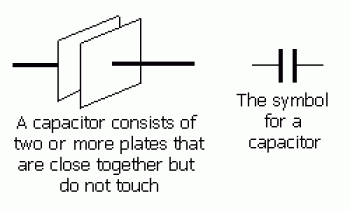 Capacitors can be large or small and the size is the result of the value of the capacitor as well as the voltage it is capable of withstanding.
There is a lot to learn about capacitors and we will only be discussing the very basics.
There are many types of capacitors, here are 5 of the most common types:
AIR - such as a tuning capacitor in a radio.
GREENCAP - a polyester capacitor.
CERAMIC - a ceramic insulating material that produces a very compact
capacitor
MONOBLOCK - also called monolithic - a multi-cceramic capacitor
ELECTROLYTIC - aluminium plates with a moist insulating medium. This type of capacitor has a very high capacitance in a small space.
The diagram below shows a single-ended electrolytic, suitable for mounting on a printed circuit board and the symbol.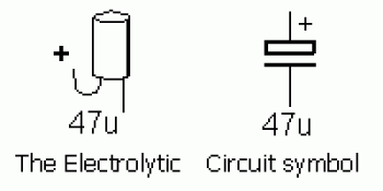 The unit for capacitance is the FARAD. But one Farad is an enormous value and we don't use values this large in electronics. The value we use is the micro-farad. A microfarad is one-millionth of a farad.
For some circuits we need capacitors of more than 1 microfarad capacitance and for others we need less than 1 microfarad.
For a power supply we need electrolytics of 10 microfarad, 100 microfarad, 1,000 microfarad and even 10,000 microfarad. The letter to signify microfarad is "uF" or simply "u". Thus 1microfarad is 1u, 10 microfarad is 10u etc.
For audio work we need smaller values such as .1microfarad and .01 microfarad.
In electronics, we try and avoid using the decimal point as it can be rubbed off components and omitted from photocopies of circuit diagrams.
To get around this we use sub-multiples and the sub-multiple of microfarad is nanofarad.
1,000 nanofarad = 1 microfarad.
Thus .1u = 100 nanofarad.
The letter to represent nanofarad is "n".
Thus .01u = 10n
For radio frequency work, even smaller values of capacitance are needed.
The nanofarad is divided into 1,000 parts called picofarad. Thus 1,000 picofarad = 1nanofarad.
The picofarad is written pF or simply "p."
Thus 1,000p = 1n.
Some capacitors are physically very small and there is very little space to write the component value. To get around this, manufacturers have produced a numbering system using 3 digits.
It is based on picofarads. A 100 picofarad capacitor is written as 101, A 1,000 picofarad capacitor is written 102, A 10 nanofarad capacitor is written 103 and 100 nanofarads is written 104. The third digit represents the number of zero's.
For example: 1n = 1,000p = 102.
10n = 10,000 = 103
100n = 100,000 = 104
Capacitors are often used in electric and electronic circuits as energy-storage devices. They can also be used to differentiate between high-frequency and low-frequency signals. This property makes them useful in electronic filters. Practical capacitors have series resistance, internal leakage of charge, series inductance and other non-ideal properties not found in a theoretical, ideal, capacitor.
The capacitor is used in almost every electronic circuit. It is a very important component and it does many different things, depending on where it is placed.
A capacitor is basically a device that stores a charge of electricity.
It has two or more plates that are separated by air or a non conducting medium such as plastic.
A basic capacitor is shown in the diagram below with the corresponding circuit symbol.

There is a lot to learn about capacitors and we will only be discussing the very basics.
There are many types of capacitors, here are 5 of the most common types:
AIR - such as a tuning capacitor in a radio.
GREENCAP - a polyester capacitor.
CERAMIC - a ceramic insulating material that produces a very compact
capacitor
MONOBLOCK - also called monolithic - a multi-cceramic capacitor
ELECTROLYTIC - aluminium plates with a moist insulating medium. This type of capacitor has a very high capacitance in a small space.
The diagram below shows a single-ended electrolytic, suitable for mounting on a printed circuit board and the symbol.

For some circuits we need capacitors of more than 1 microfarad capacitance and for others we need less than 1 microfarad.
For a power supply we need electrolytics of 10 microfarad, 100 microfarad, 1,000 microfarad and even 10,000 microfarad. The letter to signify microfarad is "uF" or simply "u". Thus 1microfarad is 1u, 10 microfarad is 10u etc.
For audio work we need smaller values such as .1microfarad and .01 microfarad.
In electronics, we try and avoid using the decimal point as it can be rubbed off components and omitted from photocopies of circuit diagrams.
To get around this we use sub-multiples and the sub-multiple of microfarad is nanofarad.
1,000 nanofarad = 1 microfarad.
Thus .1u = 100 nanofarad.
The letter to represent nanofarad is "n".
Thus .01u = 10n
For radio frequency work, even smaller values of capacitance are needed.
The nanofarad is divided into 1,000 parts called picofarad. Thus 1,000 picofarad = 1nanofarad.
The picofarad is written pF or simply "p."
Thus 1,000p = 1n.
Some capacitors are physically very small and there is very little space to write the component value. To get around this, manufacturers have produced a numbering system using 3 digits.
It is based on picofarads. A 100 picofarad capacitor is written as 101, A 1,000 picofarad capacitor is written 102, A 10 nanofarad capacitor is written 103 and 100 nanofarads is written 104. The third digit represents the number of zero's.
For example: 1n = 1,000p = 102.
10n = 10,000 = 103
100n = 100,000 = 104
2 Way Cross-Over 3500 Hz (bass and treble)
This is 2 way cross-over for your speaker system. This circuit will handle 2 speaker that are woofer (low frequency) an tweeter (high frequency).
The result will shown as below picture:
 Here the schematic diagram of the circuit:

The result will shown as below picture:
 Here the schematic diagram of the circuit:
Tuesday, March 31, 2009
Audio Clipping indicator.
It's possible to build a clipping indicator like accesory for amplifier which detects amplifier limitation, when output transistors are fully opened and signal is cutted close to power supply voltage. In this case is acoustic signal distorted in a power amplifier. Circuit as usually is from authors pages. I redraw them in a Eagle and I designed circuit board for two channels. I added place for two LEDs for power supply voltage indicators. This board have small pads, which is not much good. Eagle has these pads too small in default state.
Download this schematic
Semiconductor list datasheet download. (PDF Format)
1. BC639
2. BC640
Schematics diagram

Download this schematic
1. BC639
2. BC640
Testing
First we must to test power supply part. Fuses F2 to F5 we leave out and for sure we check again circuit of rectifier and capacitor polarity. a zkontrolujeme pro jistotu zapojení usměrňovače a polaritu kondenzátorů. Possible error can be fatal. If is all OK, that on capacitors will be voltage about 51V. Exact voltage depends on used transformer and power line voltage. After disconnecting will be voltage on capacitor for a long time. We can discharge them with a resistor 100R 2W. It's possible, that with power-on blows fuse F1 even all is OK. In my situation is charging current too big, that I had place NTC thermistor in a series with primary transformer side. I get them from old PC power supply, where it has identical function. Better idea is to use "soft start" circuit, which is made from big resistor on primary side of transformer and relay, which short-circuit resistor after few seconds. I didn't found any circuit which I liked it.
When the power supply works correctly, we can go to test amplifier. First we set trmmer P1 to one end position with maximum resistance. In to the fuse holders for one channel we place resistors 100R 1/4W. With disconnected output and input we can power-on amplifier. On the resistor we would measure maximally 2.5V, which matches current 25mA. If is everything allright, we wait for discharging after power-off and replace resistor with fuses. Initially for testing we can use smaller values. I had switched two wires from power transistors on one channel and resistors smokes and smells. Really is better to everything double check.
Now we must set the bias current. Use amperemeter in place of F2. Turn the trimmer P1, until is current 100mA. How amplifier warming-up current is changing. Regulate current value when it is stabilized, which can be after 15 minutes. Identical procedure repeat for second channel.
With disconnected input we can measure DC offset on the output. In my example I measured 19mV on left channel and 22mV on right channel.
Now we can made regular tests and connects speakers and signal source. I tested with connecting of the amplifier input directly on the output of soundcard. You must carefully increase volume, because amplifier has enough power to destroy small speakers.
Monday, March 30, 2009
Power supply for the 40 W single chip amplifier.
Constructing the power supply for this amplifier is simple. As shown on the schematic above you need to wire up a 18-0-18 (center tapped) transformer in order to get the recommended +/- 25V. Be very careful since this construction involves mains wiring.


1-chip 40 watt amplifier.
This is a compact, easy to build amplifier that uses one IC only but delivers 40 watts of audio power. It is ideal for amplifying audio from your mobile CD player or iPod. The chip being used here is the TDA1514 originally brought to the market by Phillips/Valvo. The best characteristics of this chip is its high output power and robustness. It is available in a 9-pin SIL plastic package with a metal mount.
For a single channel amplifier(mono), a 80 VA transformer (T1) should be sufficient. If you construct two channels (or stereo) amps, 120 VA is recommended. Capacitors Cx and Cy should be at least 4.700uF rated at 35V. It can be up to 10.000uF. Capacitors twice as large discharge slower giving better peak power potential resulting to better power output. Feel free to increase the capacitance but take note that you may not get much additional benefit for the price involved. Make sure they are connected the right way around too or they will blow and cause injury.

Download this schematic diagram.
Semiconductor datasheet component. (PDF Format)
1. TDA 1514
Its package has a heat resistance of less than 1.5K/W. This means that the heatsink must have a heat resistance of only 3.8K/W when the chip reaches its maximum power dissipation of 19W (at Ub = +/-27.5V, Tu = 500C).
One can see from the diagram that only a handful of passive elements are needed to build the chip into a powerful audio amplifier. The power supply as supplied must be able to deliver a current of at least 3 amperes. The standby current consumption is about 60 mA. The supply voltage must never go beyond 27.5 volts!
For a single channel amplifier(mono), a 80 VA transformer (T1) should be sufficient. If you construct two channels (or stereo) amps, 120 VA is recommended. Capacitors Cx and Cy should be at least 4.700uF rated at 35V. It can be up to 10.000uF. Capacitors twice as large discharge slower giving better peak power potential resulting to better power output. Feel free to increase the capacitance but take note that you may not get much additional benefit for the price involved. Make sure they are connected the right way around too or they will blow and cause injury.

Download this schematic diagram.
Semiconductor datasheet component. (PDF Format)
1. TDA 1514
Subscribe to:
Posts (Atom)